GPIO
Introduction
GPIO, the General-Purpose Input/Output, A generic pin that can be dynamically configured and controlled during software operation. RK3399 has 5 groups of GPIO Banks: GPIO0~GPIO4, and each group is identified by A0~A7, B0~B7, C0~C7, and D0~D7(Not all Banks have full Numbers. For example, GPIO4 only has C0~C7 and D0~D2). Some GPIO after power on the initial state is the input mode, can be set through the software to pull up or down, can also be set as the interrupt foot, drive intensity is programmable.
In addition to common input and output functions, each GPIO port may have other reuse functions, such as GPIO2_A2, which can be utilized as follows:
GPIO2_A2
CIF_D2
The driving current, pull up and down and the initial state after reset of each GPIO port are different. Please refer to Chapter 10 GPIO in “Chapter 10” in “RK3399 Specification” for details. The GPIO driver for RK3399 is implemented in the following pinctrl file:
kernel/drivers/pinctrl/pinctrl-rockchip.c
At its core are methods and parameters that populate GPIO bank and call gpiochip_add to register with the kernel.
This paper takes GPIO0_B2 (the first sort number 1 of double-row 30Pin extension interface) and GPIO0_A3(the first sort number 2 of double-row 30Pin extension interface) as examples to write a driver for simple operation of GPIO port. The path in SDK is:
kernel/drivers/gpio/gpio-firefly.c
Here’s an example of how GPIO works with this driver.
Input and output
First, add the resource description of the driver in the DTS file:
kernel/arch/arm64/boot/dts/rockchip/rk3399-firefly-demo.dtsi
gpio_demo: gpio_demo {
    status = "okay";
    compatible = "firefly,rk3399-gpio";
    firefly-gpio = <&gpio0 10 GPIO_ACTIVE_HIGH>;          /* GPIO0_B2 */
    firefly-irq-gpio = <&gpio0 4 IRQ_TYPE_EDGE_RISING>;  /* GPIO0_A3 */
};
A pin is defined here as a general output input port:
firefly-gpio GPIO0_B2
The description of pins in DTS of AIO-3399C is different from Firefly RK3288. GPIO0_B2 is described as: <&gpio0, 10 GPIO_ACTIVE_HIGH>. The 10 here comes from: 8+2=10. Where 8 is because GPIO0_B2 belongs to group B of GPIO0, 0 if it is group A, 16 if it is group C, 24 if it is group D, and so on, and 4 is because of the 4 following B4.
GPIO_ACTIVE_HIGH indicates that the high level is valid, and if you want the low level to be valid, you can change it to: GPIO_ACTIVE_LOW, which will be read by the driver.
Then, in the probe function, the resources added by DTS are parsed. The code is as follows:
static int firefly_gpio_probe(struct platform_device *pdev)
{
    int ret; int gpio; enum of_gpio_flags flag;
    struct firefly_gpio_info *gpio_info;
    struct device_node *firefly_gpio_node = pdev->dev.of_node;

    printk("Firefly GPIO Test Program Probe\n");
    gpio_info = devm_kzalloc(&pdev->dev,sizeof(struct firefly_gpio_info *), GFP_KERNEL);
    if (!gpio_info) {
        return -ENOMEM;
    }
    gpio = of_get_named_gpio_flags(firefly_gpio_node, "firefly-gpio", 0, &flag);
    if (!gpio_is_valid(gpio)) {
        printk("firefly-gpio: %d is invalid\n", gpio); return -ENODEV;
    }
    if (gpio_request(gpio, "firefly-gpio")) {
        printk("gpio %d request failed!\n", gpio);
        gpio_free(gpio);
        return -ENODEV;
    }
    gpio_info->firefly_gpio = gpio;
    gpio_info->gpio_enable_value = (flag == OF_GPIO_ACTIVE_LOW) ? 0:1;
    gpio_direction_output(gpio_info->firefly_gpio, gpio_info->gpio_enable_value);
    printk("Firefly gpio putout\n");
    ......
}
Of_get_named_gpio_flags() reads the gpio configuration number and flag in firefly-gpio and firefly-irq-gpio from the device tree, gpio_is_valid() determines whether the GPIO number is valid, and gpio_request() applies for occupying the GPIO. If the initialization process goes wrong, you need to call gpio_free() to release the previously requested and successful GPIO.A call to gpio_direction_output() in the driver sets whether the output is high or low, where the default output is the effective level GPIO_ACTIVE_HIGH obtained from DTS. If the drive is working normally, the corresponding pin can be measured with a multimeter and should be GPIO_ACTIVE_HIGH. In practice, if you want to read GPIO, you need to set it to input mode first, and then read the value:
int val;
gpio_direction_input(your_gpio);
val = gpio_get_value(your_gpio);
The following are common GPIO API definitions:
#include <linux/gpio.h>
#include <linux/of_gpio.h>

enum of_gpio_flags {
     OF_GPIO_ACTIVE_LOW = 0x1,
};
int of_get_named_gpio_flags(struct device_node *np, const char *propname,
int index, enum of_gpio_flags *flags);
int gpio_is_valid(int gpio);
int gpio_request(unsigned gpio, const char *label);
void gpio_free(unsigned gpio);
int gpio_direction_input(int gpio);
int gpio_direction_output(int gpio, int v);
Interrupt
In Firefly’s example program, an interrupt pin is also included. The interrupt of GPIO port is similar to the input and output of GPIO. Firstly, the resource description of the driver is added in the DTS file:
kernel/arch/arm64/boot/dts/rockchip/rk3399-firefly-port.dtsi
&gpio_demo {
    ...
    firefly-irq-gpio = <&gpio0 3 IRQ_TYPE_EDGE_RISING>;  /* GPIO0_A3 */
    ...
};
IRQ_TYPE_EDGE_RISING indicates that the interrupt is triggered by the rising edge, and the interrupt function can be triggered when the pin receives the rising edge signal.
It can also be configured as follows:
IRQ_TYPE_NONE         //Default, no interrupt trigger type defined
IRQ_TYPE_EDGE_RISING  //Edge trigger
IRQ_TYPE_EDGE_FALLING //Drop trigger
IRQ_TYPE_EDGE_BOTH    //Edge trigger or Drop trigger
IRQ_TYPE_LEVEL_HIGH   //High level trigger
IRQ_TYPE_LEVEL_LOW    //Low level trigger
Then, in the probe function, we will analyze the resources added by DTS, and then make the interrupt registration application. The code is as follows:
static int firefly_gpio_probe(struct platform_device *pdev)
{
    int ret; int gpio; enum of_gpio_flags flag;
    struct firefly_gpio_info *gpio_info;
    struct device_node *firefly_gpio_node = pdev->dev.of_node;
    ...
    gpio_info->firefly_irq_gpio = gpio;
    gpio_info->firefly_irq_mode = flag;
    gpio_info->firefly_irq = gpio_to_irq(gpio_info->firefly_irq_gpio);
    if (gpio_info->firefly_irq) {
        if (gpio_request(gpio, "firefly-irq-gpio")) {
           printk("gpio %d request failed!\n", gpio); gpio_free(gpio); return IRQ_NONE;
        }
        ret = request_irq(gpio_info->firefly_irq, firefly_gpio_irq, flag, "firefly-gpio", gpio_info);
        if (ret != 0) free_irq(gpio_info->firefly_irq, gpio_info);
            dev_err(&pdev->dev, "Failed to request IRQ: %d\n", ret);
    }
    return 0;
}
static irqreturn_t firefly_gpio_irq(int irq, void *dev_id) //The interrupt function
{
    printk("Enter firefly gpio irq test program!\n"); return IRQ_HANDLED;
}
Call gpio_to_irq() to convert the PIN value of GPIO into the corresponding IRQ value, call gpio_request() to apply for the IO port, call request_irq() to apply for interrupt, if failure to call free_irq() to release, in this function, gpio_info->firefly_irq is the hardware interrupt number to be applied. Firefly_gpio_irq () is the interrupt function, gpio_info->firefly_irq_mode is the attribute of interrupt processing, *”firefly-gpio” *is the device driver name, gpio_info is the device structure of the device, which will be used to register the Shared interrupt.
Multiplex
How do you define what features of GPIO are reusable and how do you switch between them at run time? Take I2C4 as an example to make a simple introduction.
According to the specification table, the functions of I2C4_SDA and I2C4_SCL are defined as follows:
Pad# 	                func0 	        func1
I2C4_SDA/GPIO1_B3 	gpio1b3 	i2c4_sda
I2C4_SCL/GPIO1_B4 	gpio1b4 	i2c4_scl
In kernel/arch/arm64/boot/dts/rockchip/rk3399.dtsi:
i2c4: i2c@ff3d0000 {
    compatible = "rockchip,rk3399-i2c";
    reg = <0x0 0xff3d0000 0x0 0x1000>;
    clocks = <&pmucru SCLK_I2C4_PMU>, <&pmucru 	PCLK_I2C4_PMU>;
    clock-names = "i2c", "pclk";
    interrupts = <GIC_SPI 56 IRQ_TYPE_LEVEL_HIGH 0>;
    pinctrl-names = "default", "gpio";
    pinctrl-0 = <&i2c4_xfer>;
    pinctrl-1 = <&i2c4_gpio>;
    #address-cells = <1>;
    #size-cells = <0>;
    status = "disabled";
};
Here, the properties at the beginning of pinctrl- are relevant to reuse control:
pinctrl-names : Defines the state name list default (i2c function) and gpio two states.
pinctrl-0 : Defines the pinctrl: &i2c4_xfer that needs to be set when state 0 (default) is defined.
pinctrl-1 : Defines the pinctrl: &i2c4_gpio that needs to be set when state 1 (gpio) is defined.
These pinctrl in kernel/arch/arm64 / boot/DTS/rockchip/rk3399.dtsi file in such definition:
pinctrl: pinctrl {
    compatible = "rockchip,rk3399-pinctrl";
    rockchip,grf = <&grf>;
    rockchip,pmu = <&pmugrf>;
    #address-cells = <0x2>;
    #size-cells = <0x2>;
    ranges;
    i2c4 {
    i2c4_xfer: i2c4-xfer {
        rockchip,pins = <1 12 RK_FUNC_1 &pcfg_pull_none>, <1 11 RK_FUNC_1 &pcfg_pull_none>;
    };
    i2c4_gpio: i2c4-gpio {  //此段源码未添加,只做参考例子
        rockchip,pins = <1 12 RK_FUNC_GPIO &pcfg_pull_none>, <1 11 RK_FUNC_GPIO &pcfg_pull_none>;
    };
};
RRK_FUNC_1 and RK_FUNC_GPIO are defined in kernel/include/dt-bindings/pinctrl/rk.h:
 #define RK_FUNC_GPIO    0
 #define RK_FUNC_1   1
 #define RK_FUNC_2   2
 #define RK_FUNC_3   3
 #define RK_FUNC_4   4
 #define RK_FUNC_5   5
 #define RK_FUNC_6   6
 #define RK_FUNC_7   7
n addition, values like “1 11” and “1 12” are encoded in the same way as described in “Input/Output” in the previous section, “1 11” for GPIO1_B3 and “1 12” for GPIO1_B4.
In reuse, if “default” (i2c function) is selected, the pinctrl of i2c4_xfer will be applied, and the two pins GPIO1_B3 and GPIO1_B4 will be switched to the corresponding i2c function. If “gpio” is selected, the pinctrl of i2c4_gpio will be applied to restore the two pins of GPIO1_B3 and GPIO1_B4 to the function of gpio.
Let’s see how kernel/drivers/i2c/ i2c/busses/i2c-rockchip.c switches and reuses functions:
static int rockchip_i2c_probe(struct platform_device *pdev)
{
    struct rockchip_i2c *i2c = NULL; struct resource *res;
    struct device_node *np = pdev->dev.of_node; int ret;//
    ...
    i2c->sda_gpio = of_get_gpio(np, 0);
    if (!gpio_is_valid(i2c->sda_gpio)) {
        dev_err(&pdev->dev, "sda gpio is invalid\n");
        return -EINVAL;
    }
    ret = devm_gpio_request(&pdev->dev, i2c->sda_gpio, dev_name(&i2c->adap.dev));
    if (ret) {
        dev_err(&pdev->dev, "failed to request sda gpio\n");
        return ret;
    }
    i2c->scl_gpio = of_get_gpio(np, 1);
    if (!gpio_is_valid(i2c->scl_gpio)) {
        dev_err(&pdev->dev, "scl gpio is invalid\n");
        return -EINVAL;
    }
    ret = devm_gpio_request(&pdev->dev, i2c->scl_gpio, dev_name(&i2c->adap.dev));
    if (ret) {
        dev_err(&pdev->dev, "failed to request scl gpio\n");
        return ret;
    }
    i2c->gpio_state = pinctrl_lookup_state(i2c->dev->pins->p, "gpio");
    if (IS_ERR(i2c->gpio_state)) {
        dev_err(&pdev->dev, "no gpio pinctrl state\n");
        return PTR_ERR(i2c->gpio_state);
    }
    pinctrl_select_state(i2c->dev->pins->p, i2c->gpio_state);
    gpio_direction_input(i2c->sda_gpio);
    gpio_direction_input(i2c->scl_gpio);
    pinctrl_select_state(i2c->dev->pins->p, i2c->dev->pins->default_state);
    // ...
}
First, of_get_gpio() is called to extract the gpios of i2c4 node in the device tree belonging to the defined two gpios:
gpios = <&gpio1 GPIO_B3 GPIO_ACTIVE_LOW>, <&gpio1 GPIO_B4 GPIO_ACTIVE_LOW>;
devm_gpio_request () is then called to apply for gpio, followed by pinctrl_lookup_state () to find the “gpio” state, and the default state “default” is already saved by the framework into i2c->dev-pins->default_state.
Finally, pinctrl_select_state () is called to select whether it is “default” or “gpio”.
The following are common reuse API definitions:
#include <linux/pinctrl/consumer.h>
struct device {
    //...
    #ifdef CONFIG_PINCTRL
    struct dev_pin_info	*pins;
    #endif
    //...
};
struct dev_pin_info {
    struct pinctrl *p;
    struct pinctrl_state *default_state;
    #ifdef CONFIG_PM
    struct pinctrl_state *sleep_state;
    struct pinctrl_state *idle_state;
    #endif
};
struct pinctrl_state * pinctrl_lookup_state(struct pinctrl *p, const char *name);
int pinctrl_select_state(struct pinctrl *p, struct pinctrl_state *s);
IO-Domain
In complex SOC, the designer will generally divide the Power supply of the system into several independent blocks, which is called Power Domain. This has many advantages, such as:
The voltage Domain is uniformly configured at the DTS node of IO-Domain, which does not require each driver to be configured once for easy management.
In accordance with the Upstream approach, it is more convenient to Upstream if necessary in the future;
The Regulator of IO-Domain supports dynamic regulation of voltage field during operation. For example, a Regulator of PMIC can be dynamically switched between 1.8v and 3.3v. If the Regulator voltage changes, the Regulator will notify the driver of IO-Domain to reset the voltage field.
The Power Domain Map table on ROC-3399-PC-PLUS schematic diagram and its configuration are shown in the following table:
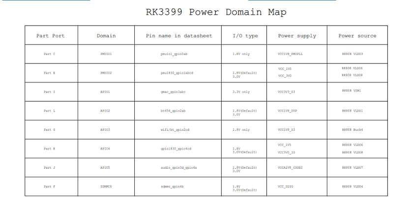
It can be seen from the schematic diagram of RK3399 SDK that the voltage field of bt656-supply is connected with vcc18_dvp, and vcc_io comes from VLDO1 of PMIC RK808. vcc1v8_dvp can be found in DTS, and bt656-supply = <&vcc18_dvp>.
The configuration of other channels is similar. It should be noted that Regulator would be different if there were other PMIC and would be regulated by the actual circuit.
Debug method
IO instruction
GPIO debugging has a very useful tool, that is IO instruction, ROC-3399-PC-PLUS Android system default has built-in IO instruction, IO instruction can be used to read or write the status of each IO port in real time, here is a brief introduction to the use of IO instruction. First look at IO instruction help
#io --help
Unknown option: ?
Raw memory i/o utility - $Revision: 1.5 $

io -v -1|2|4 -r|w [-l <len>] [-f <file>] <addr> [<value>]

   -v         Verbose, asks for confirmation
   -1|2|4     Sets memory access size in bytes (default byte)
   -l <len>   Length in bytes of area to access (defaults to
              one access, or whole file length)
   -r|w       Read from or Write to memory (default read)
   -f <file>  File to write on memory read, or
              to read on memory write
   <addr>     The memory address to access
   <val>      The value to write (implies -w)

Examples:
   io 0x1000                  Reads one byte from 0x1000
   io 0x1000 0x12             Writes 0x12 to location 0x1000
   io -2 -l 8 0x1000          Reads 8 words from 0x1000
   io -r -f dmp -l 100 200    Reads 100 bytes from addr 200 to file
   io -w -f img 0x10000       Writes the whole of file to memory

Note access size (-1|2|4) does not apply to file based accesses.
As can be seen from the help, if you want to read or write a register, you can use:
io -4 -r 0x1000 //Read the value of the 4-bit register starting at 0x1000
io -4 -w 0x1000 //Write the value of the 4-bit register starting at 0x1000
Example:
See the reuse of GPIO1_B3 pins.
From the datasheet of the main control, the corresponding register base address of GPIO1 was found to be 0xff320000.
The offset of GPIO1B_IOMUX from the datasheet of the master control is 0x00014.
GPIO1_B3 iomux register address is: Operational Base + offset =0xff320000+0x00014=0xff320014.
Check the reuse of GPIO1_B3 with the following instructions:
# io -4 -r 0xff320014
ff320014:  0000816a
From datasheet, we found[7:6]:
gpio1b3_sel
GPIO1B[3] iomux select
2'b00: gpio
2'b01: i2c4sensor_sda
2'b10: reserved
2'b11: reserved
Therefore, it can be determined that the GPIO is reused as i2c4sensor_sda.
If you want to reuse as GPIO, you can use the following instructions:
# io -4 -w 0xff320014 0x0000812a
GPIO debuge interface
Debugfs filesystems are designed to provide developers with more kernel data for easy debugging. GPIO debugging can also use the Debugfs filesystem here for more kernel information. GPIO’s interface to the Debugfs file system is /sys/kernel/debug/ GPIO, and information about this interface can be read as follows:
# cat /sys/kernel/debug/gpio
GPIOs 0-31, platform/pinctrl, gpio0:
 gpio-2   (                    |vcc3v3_3g           ) out hi
 gpio-4   (                    |bt_default_wake_host) in  lo
 gpio-5   (                    |power               ) in  hi
 gpio-9   (                    |bt_default_reset    ) out lo
 gpio-10  (                    |reset               ) out lo
 gpio-13  (                    |?                   ) out lo

GPIOs 32-63, platform/pinctrl, gpio1:
 gpio-32  (                    |vcc5v0_host         ) out hi
 gpio-34  (                    |int-n               ) in  hi
 gpio-35  (                    |vbus-5v             ) out lo
 gpio-45  (                    |pmic-hold-gpio      ) out hi
 gpio-49  (                    |vcc3v3_pcie         ) out hi
 gpio-54  (                    |mpu6500             ) out hi
 gpio-56  (                    |pmic-stby-gpio      ) out hi

GPIOs 64-95, platform/pinctrl, gpio2:
 gpio-83  (                    |bt_default_rts      ) in  hi
 gpio-90  (                    |bt_default_wake     ) in  lo
 gpio-91  (                    |?                   ) out hi

GPIOs 96-127, platform/pinctrl, gpio3:
 gpio-111 (                    |mdio-reset          ) out hi

GPIOs 128-159, platform/pinctrl, gpio4:
 gpio-149 (                    |hp-con-gpio         ) out lo
As can be seen from the information read, the kernel lists the current state of GPIO. Taking GPIO0 group as an example, gpio-2(GPIO0_A2) serves as the power control pin of 3G module (vcc3v3_3g) and outputs the high level (out hi).
FAQs
Q1: How do I switch the MUX value of PIN to a generic GPIO?
A1 : When using GPIO request, the MUX value of the PIN is forced to switch to GPIO, so make sure that the PIN PIN is not used by other modules when using the PIN PIN for GPIO function.
Q2: Why have I read out the values with IO instructions for 0x00000000?
A2 : If you use the IO command to read a GPIO register, the read value is abnormal, such as 0x00000000 or 0xffffffff. Please confirm whether CLK of GPIO is turned off or not. CLK of GPIO is controlled by CRU. You can check whether CLK is turned on by reading CRU_CLKGATE_CON register under datasheet. If not, you can use the IO command to set up the corresponding register to open the CLK. After opening the CLK, you should be able to read the correct register value.
Q3: The voltage of PIN PIN measured is wrong. How should I check it?
A3 : When the voltage of the PIN is not measured correctly, if external factors are excluded, it can be confirmed whether the IO voltage source where the PIN is located is correct and whether the IO-Domain configuration is correct.
Q4: What is the difference between gpio_set_value() and gpio_direction_output()?
A4 : If the GPIO is not used to dynamically switch input and output, it is recommended to set the GPIO output direction at the beginning, and use the gpio_set_value() interface when pulling up and down later, rather than the gpio_direction_output() interface. Because there is a mutex lock in the gpio_direction_output() interface, there will be an error exception to the interrupt context call, and compared with gpio_set_value(), gpio_direction_output() does more things and wastes resources.。